
Page 600 - Engineering Digital Design
P. 600
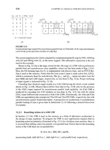
570                              CHAPTER 12 / MODULE AND BIT-SLICE DEVICES


                  CL LD     PRE CLR
                  1  X   X    0    1       xLD-P,                    \LD-Pj
                                          CL\ 00    01   11   10     CL\  00  01   11   10
                                          /•M X
                  00    0     0    0
                  0   0  1    0    0        0   0    0  CD    0       0   0    0    0  p~
                  0   1  0    0   1          1  0    0    0   0        1  (1   1    1   1)
                  0   1  1    1    0
                                                                / PRE                     / CLH
                    X = Irrelevant input
                          (a)                                       (b)

                    FIGURE 12.9
                    Combinational logic required for asynchronous parallel load, (a) Truth table, (b) K-maps and minimum
                    cover for the preset and clear overrides of a flip-flop.


                    The second expression for CLR is obtained by complementing the K-map for PRE, ANDing
                    with LD and ORing with CL, as the terms suggest. This alternative expression is the one
                    used in this example.
                       Shown in Fig. 12.10a is the logic circuit for the 7th stage of a USR with asynchronous
                    parallel load and asynchronous clear capability, where use has been made of Eqs. (12.4).
                    Here, the NS-forming logic for Dj is implemented with discrete logic, and an FET D flip-
                    flop is used as the memory. Notice that the load control input is made active low, LD(L),
                    which is commonly done for such devices. The Qj+\ and Qj-\ inputs are taken from the
                    next MSB and next LSB stages, respectively, as was done in Fig. 12.6a. Proper buffering
                    of input signals is indicated in Fig. 12.10a.
                       Cascading four identical stages results in a 4-bit USR having the block circuit symbol
                    shown in Fig. 12.1 Ob. Observe that it differs from that in Fig. 12.6b only by the presence
                    of the LD(L) input required for asynchronous parallel load capability. An 8-bit USR is
                    produced by cascading two 4-bit modules as was done in Fig. 12.8, but with the added
                    LD(L) input buffered and connected to both 4-bit USRs. Functionally, the 4-bit and 8-bit
                    USRs are equivalent to the commercial 74xxl94 and 74xx299 USRs, respectively, but with
                    asynchronously parallel loaded data inputs. A perspective on synchronous vs asynchronous
                    parallel loading of data is given later in Subsection 12.3.6 following a detailed discussion
                    of counters.


                    12.2.5 Branching Action of a 4-Bit USR
                    In Section 13.3 the USR is used as the memory as a form of alternative architecture in
                    the design of state machines. To program the USR in such applications requires that its
                    branching action be labeled as illustrated in Fig. 12.11 for a fictitious state machine. Here, it
                    is assumed that shifting action has priority over parallel load. Notice that for the branching
                    action of the USR there are six possibilities:

                                           H, SLO, SL1, SRO, SRI, and PL,

                    representing hold, shift left 0 or 1, shift right 0 or 1, and parallel load, respectively.