
Page 596 - Engineering Digital Design
P. 596
566 CHAPTER 12 / MODULE AND BIT-SLICE DEVICES
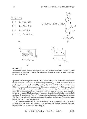
0 0 True Hold
0 1 Q J+1 Right Shift
1 0 Qj.., Left Shift
1 1 P, Parallel load
(a) (b)
(c) (d)
FIGURE 12.5
Design of a 1-bit slice universal shift register (USR). (a) Operation table for the Jth stage, (b) State
diagram for the Jth stage, (c) NS logic K-map plotted from (b) assuming the use of D flip-flops.
(d)MUX K-map for Dj.
operation. The state diagram for the 7th stage, shown in Fig. 12.5b, is obtained directly from
the operation table. For example, the branching condition f ab is the Boolean sum of all set
producing conditions, each formed by ANDing the mode controls with its corresponding
NS action parameter. Thus, since a set condition can be introduced by a shift right operation,
the term S\So • QJ+\ must be included in the expression for /„/,. Because a left shift or a
parallel load can also introduce a set condition into the register, two more terms are added
for a total of three ANDed terms in the expression f ab as indicated. Similarly, the set hold
condition fb must include S\ SQ • Qj (the true hold condition) as well as all the set terms in
f ab. The two remaining branching conditions, f\, a and / a, can be found from the sum rule,
but are irrelevant for a D flip-flop design.
The minimum NS logic for the 7th stage is obtained from the K-map in Fig. 12.5c, which
is plotted from the state diagram in Fig. 12.5b, assuming the use of D flip-flops. The logic
expression for Dj , as read from the K-map, is
(12.2)