
Page 595 - Engineering Digital Design
P. 595
12.2 REGISTERS 565
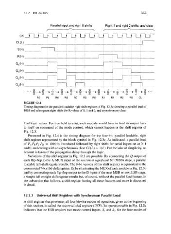
Parallel input and right 0 shifts Right 1 and right 0 shifts, and clear
CK
CL(L)
S(H)
R(H)
QA<H).
Q B(H)
Q C(H)
Q D(H)
RO PL RO RO RO RO RO R1 R1 RO RO CL
FIGURE 12.4
Timing diagram for the parallel loadable right shift register of Fig. 12.3c showing a parallel load of
1010 and subsequent right shifts for R values of 0, 1 and 0, and asynchronous clear.
load logic values. For true hold to exist, each module would have to feed its output back
to itself on command of the mode control, which cannot happen in the shift register of
Fig. 12.3.
Presented in Fig. 12.4 is the timing diagram for the four-bit, parallel loadable, right
shift register represented by the block symbol in Fig. 12.3c. As indicated, a parallel load
of P APBPcPo = 1010 is introduced followed by right shifts for serial inputs set at 0, 1
and 0, and ending with an asynchronous clear CL(L) = 1(L). For the sake of simplicity, no
account is taken of the propagation delay through the logic.
Variations of the shift register in Fig. 12.3 are possible. By connecting the Q output of
each flip-flop to the /o MUX input of the next most significant bit (MSB) stage, a parallel
loadable left-shift register results. The 8-bit version of this shift register is equivalent to the
commercial 74xxl66 shift register. Or by eliminating the MUX of each module in Fig. 12.3b
and by connecting each flip-flop output to the D input of the next MSB or next LSB stage,
a simple left or right shift register results but, of course, without the parallel load feature. In
the subsection that follows, a shift register having all these features and more is discussed
in detail.
12.2.3 Universal Shift Registers with Synchronous Parallel Load
A shift register that possesses all four bitwise modes of operation, given at the beginning
of this section, is called the universal shift register (USR). Its operation table in Fig. 12.5a
indicates that the USR requires two mode control inputs, S\ and So, for the four modes of