
Page 593 - Engineering Digital Design
P. 593
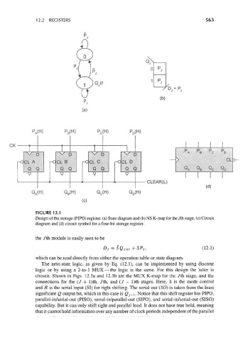
12.2  REGISTERS                                                      563


                 P A(H)       P B(H)       P C(H)       P D(H)


                                                                              p    p    p   p
                                                                              r    r   r    r
                                                                              A    B    C   O
                                                                                              CL>-


                                                               CLEAR(L)
                                                                                      (d)
                 Q A(H)       Q B(H)       Q C(H)       Q D(H)
                                     (c)
                  FIGURE 12.1
                  Design of the storage (PIPO) register, (a) State diagram and (b) NS K-map for the Jth stage, (c) Circuit
                  diagram and (d) circuit symbol for a four-bit storage register.


                  the Jth module is easily seen to be
                                             Dj= SQ J+[ +SPj,                        (12.1)

                  which can be read directly from either the operation table or state diagram.
                    The next-state logic, as given by Eq. (12.1), can be implemented by using discrete
                  logic or by using a 2-to-l MUX — the logic is the same. For this design the latter is
                  chosen. Shown in Figs. 12.3a and 12.3b are the MUX K-map for the Jth stage, and the
                  connections for the (/ + l)th, 7th, and (J — l)th stages. Here, S is the mode control
                  and R is the serial input (SI) for right shifting. The serial out (SO) is taken from the least
                  significant Q output bit, which in this case is Qj-\. Notice that this shift register has PIPO,
                  parallel-in/serial-out (PISO), serial-in/parallel-out (SIPO), and serial-in/serial-out (SISO)
                  capability. But it can only shift right and parallel load. It does not have true hold, meaning
                  that it cannot hold information over any number of clock periods independent of the parallel