
Page 594 - Engineering Digital Design
P. 594
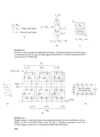
f  =  SO + SP
                       Q J+1 - Right shift input  ab  J+1   J

                       Pj- Parallel load input

                              (a)


                     FIGURE 12.2
                     Design of a 1-bit slice parallel loadable right shift register, (a) Operation table showing mode control,
                     S, and NS action for the 7th stage, (b) State diagram derived from (a), (c) NS K-map plotted from (b)
                     assuming the use of D flip-flops.


                                               PI
                             /
                              P J+1(H)        Pj(H)
                 R(H) = SI — *
                                      1   r—         I              I
                                               I     'o
                                      'o                            'o
                             r- S             S   J        p S  J-1
                                  MUX            MUX            MUX
                                     Y              Y              Y
         s\          S(H) —                                                        p    p   p    p
                                                                                                r
                                                                                        r
                                                                                            r
                                                                                        B
                                                                                            C
          0 Q J+i     CK        • '            '               ,               .   r  A Rgt. shift register D
                                s ' D          \ /  D         \ ' D            >    with parallel load  CL  ®~
          1  P J             rC CL J+1      rC CL  J       rC CL  J-1              QA   QB  QC   QO
                /b j
                                Q    Q         Q    Q         Q    Q
                                 Y   <          Y   <          Y   • i      >
                                                                       CL(L)
             (a)                                                                           (c)
                                    Q J+1(H)       Qj(H)
                                   \                 _ , _
                                                    v
                                                    PO
                                                (b)
                     FIGURE 12.3
                     Modular design of a right shift register with synchronous parallel load and asynchronous clear ca-
                     pability. (a) Two-to-one MUX K-map for the 7th stage, (b) Modular connections for three bits.
                     (c) Block diagram symbol for the 4-bit parallel loadable right shift register.
                     564