
Page 599 - Engineering Digital Design
P. 599
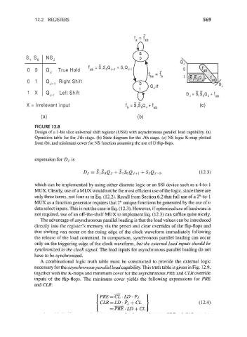
12.2  REGISTERS                                                     569


              0 0     Qj  True Hold

              0 1     Q J+1 Right Shift

              1 X     Q ,, Left Shift

              X = Irrelevant input                    f b = S^Qj + f b              (c)

                    (a)                                    (b)
                 FIGURE 12.8
                 Design of a 1-bit slice universal shift register (USR) with asynchronous parallel load capability, (a)
                 Operation table for the 7th stage, (b) State diagram for the 7th stage, (c) NS logic K-map plotted
                 from (b), and minimum cover for NS function assuming the use of D flip-flops.


                 expression for Dj is

                                                                     ,              (12.3)


                 which can be implemented by using either discrete logic or an SSI device such as a 4-to-l
                 MUX. Clearly, use of a MUX would not be the most efficient use of the logic, since there are
                 only three terms, not four as in Eq. (12.2). Recall from Section 6.2 that full use of a 2"-to-l
                 MUX as a function generator requires that 2" unique functions be generated by the use of n
                 data select inputs. This is not the case in Eq. (12.3). However, if optimized use of hardware is
                 not required, use of an off-the-shelf MUX to implement Eq. (12.3) can suffice quite nicely.
                    The advantage of asynchronous parallel loading is that the load values can be introduced
                 directly into the register's memory via the preset and clear overrides of the flip-flops and
                 that shifting can occur on the rising edge of the clock waveform immediately following
                 the release of the load command. In comparison, synchronous parallel loading can occur
                 only on the triggering edge of the clock waveform, but the external load inputs should be
                 synchronized to the clock signal. The load inputs for asynchronous parallel loading do not
                 have to be synchronized.
                    A combinational logic truth table must be constructed to provide the external logic
                 necessary for the asynchronous parallel load capability. This truth table is given in Fig. 1 2.9,
                 together with the K-maps and minimum cover for the asynchronous PRE and CLR override
                 inputs of the flip-flops. The minimum cover yields the following expressions for PRE
                 and CLR:

                                            PRE=CL-LD- Pj
                                            CLR = LD-Pj + CL                        (12.4)
                                                = PRE -LD + CL