
Page 603 - Engineering Digital Design
P. 603
12.3 SYNCHRONOUS BINARY COUNTERS 573
,
D Q -Q(H)
A
CK — > Q 0-L-Q(L)
(C)
(d)
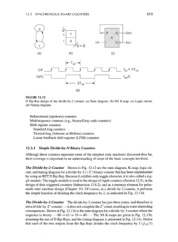
FIGURE 12.12
D flip-flop design of the divide-by-2 counter, (a) State diagram, (b) NS K-map. (c) Logic circuit,
(d) Timing diagram.
Bidirectional (up/down) counters
Multisequence counters (e.g., binary/Gray code counters)
Shift register counters
Standard ring counters
Twisted ring (Johnson or Mobius) counters
Linear feedback shift register (LFSR) counters
12.3.1 Simple Divide-by-N Binary Counters
Although these counters represent some of the simplest state machines discussed thus far,
their coverage is important to an understanding of some of the basic concepts involved.
The Divide-by-2 Counter Shown in Fig. 12.12 are the state diagram, K-map, logic cir-
l
cuit, and timing diagram for a divide-by-2 (^-2 ) binary counter that has been implemented
by using an RET D flip-flop. Because it exhibits only toggle character, it is also called a tog-
gle module. The toggle module is used in the design of ripple counters (Section 12.5), in the
design of data-triggered counters (Subsection 13.6.2), and as a memory element for pulse-
mode state machine design (Chapter 15). Of course, as a divide-by-2 counter, it performs
the simple function of dividing the clock frequency by 2, as indicated in Fig. 12.12d.
The Divide-by-3 Counter The divide-by-3 counter has just three states, and therefore is
2
M
not a divide-by-2 -counter—it does not complete the 2 count, resulting in some interesting
consequences. Shown in Fig. 12.13a is the state diagram for a divide-by-3 counter where the
sequence is binary • • • 00 -> 01 —» 10 —»• 00 • • •. The NS K-maps are given in Fig. 12.13b,
assuming the use of D flip-flops, and the timing diagram is presented in Fig. 12.13c. Notice
that each of the two outputs from the flip-flops divides the clock frequency by 3 (/ctf/3)