
Page 606 - Engineering Digital Design
P. 606
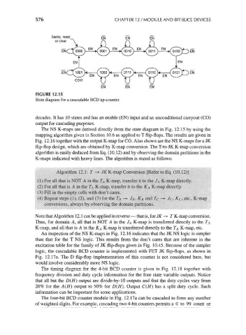
576                             CHAPTER 12 / MODULE AND BIT-SLICE DEVICES


                           Sanity, reset
                             or clear


                                                          EN       EN
                     FIGURE 12.15
                     State diagram for a cascadable BCD up-counter.


                     decades. It has 10 states and has an enable (EN) input and an unconditional carry out (CO)
                     output for cascading purposes.
                       The NS K-maps are derived directly from the state diagram in Fig. 12.15 by using the
                     mapping algorithm given in Section 10.6 as applied to T flip-flops. The results are given in
                     Fig. 12.16 together with the output K-map for CO. Also shown are the NS K-maps for a JK
                     flip-flop design, which are obtained by K-map conversion. The T-to-JK K-map conversion
                     algorithm is easily deduced from Eq. (10.12) and by observing the domain partitions in the
                     K-maps indicated with heavy lines. The algorithm is stated as follows:

                             Algorithm 12.1: T ~-> JK K-map Conversion [Refer to Eq. (10.12)]

                      (1) For all that is NOT 4 in the TA K-map, transfer it to the JA K-map directly.
                      (2) For all that is A in the TA K-map, transfer it to the KA K-map directly.
                      (3) Fill in the empty cells with don't cares.
                      (4) Repeat steps (1), (2), and (3) for the T B -* JB , KB and T c -*• /c, ^c» etc., K-map
                         conversions, always by observing the domain partitions.

                     Note that Algorithm 12.1 can be applied in reverse — that is, for JK -> T K-map conversion.
                     Thus, for domain A, all that is NOT A in the JA K-map is transferred directly to the TA
                     K-map, and all that is A in the K A K-map is transferred directly to the TA K-map, etc.
                       An inspection of the NS K-maps in Fig. 12.16 indicates that the JK NS logic is simpler
                     than that for the T NS logic. This results from the don't cares that are inherent in the
                     excitation table for the family of JK flip-flops given in Fig. 10.45. Because of the simpler
                     logic, the cascadable BCD counter is implemented with FET JK flip-flops, as shown in
                     Fig. 12.17a. The D flip-flop implementation of this counter is not considered here, but
                     would involve considerably more NS logic.
                       The timing diagram for the 4-bit BCD counter is given in Fig. 12.18 together with
                     frequency division and duty cycle information for the four state variable outputs. Notice
                     that all but the D(H) output are divide-by-10 outputs and that the duty cycles vary from
                     20% for the A(H) output to 50% for D(H). Output C(H) has a split duty cycle. Such
                     information can be important for some applications.
                       The four-bit BCD counter module in Fig. 12.17a can be cascaded to form any number
                     of weighted digits. For example, cascading two 4-bit counters permits a 0 to 99 count or