
Page 609 - Engineering Digital Design
P. 609
12.3 SYNCHRONOUS BINARY COUNTERS 579
0.1 to 9 count, etc., depending on how one views the count. Cascading three such modules
gives a 0 to 999 count. Or generally, cascading k of these modules, as in Fig. 12.17b, forms
a &-digit BCD counter with a 0 to 10^ — 1 count, where k is an integer (k = 0, 1, 2, 3, ...).
The EN input to the LSD stage is, of course, a counter enable control. If EN(H) = !(//),
the counter is enabled. But if EN(H) = Q(H), the counter is disabled and is caused to hold
in whatever state it is in at the time. The EN input can be replaced by an ANDing operation
permitting two signals to control the operation of the counter: a count enable input and an
inhibit input, both performing basically the same function.
The manner in which a cascaded BCD counter operates is as follows: Each full count of
the LSD (0) stage sends a CO signal to the next MSD (1) stage which is properly enabled on
the next rising edge of the clock pulse. Thus, for each full count (O-to-9) of stage (0), stage
(1) is bumped up 1. So after 10 such full counts of stage (0), stage (1) completes its full
count (O-to-9) and enables the next MSB stage, which is bumped up one on the next rising
edge of clock. Any output race glitches (ORGs) that occur are of no consequence, since the
single-output CO can enable the next stage only if is issued for a complete clock period.
ORG glitches occur immediately following the triggering edge of the clock waveform and
damp out long before the output CO can be picked up by the next MSB stage.
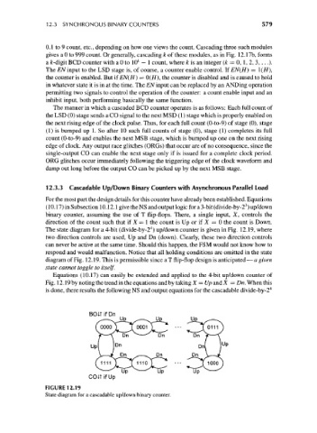
12.3.3 Cascadable Up/Down Binary Counters with Asynchronous Parallel Load
For the most part the design details for this counter have already been established. Equations
3
(10.17) in Subsection 10.12.1 give the NS and output logic for a 3-bit (divide-by-2 ) up/down
binary counter, assuming the use of T flip-flops. There, a single input, X, controls the
direction of the count such that if X = 1 the count is Up or if X = 0 the count is Down.
4
The state diagram for a 4-bit (divide-by-2 ) up/down counter is given in Fig. 12.19, where
two direction controls are used, Up and Dn (down). Clearly, these two direction controls
can never be active at the same time. Should this happen, the FSM would not know how to
respond and would malfunction. Notice that all holding conditions are omitted in the state
diagram of Fig. 12.19. This is permissible since a T flip-flop design is anticipated — a given
state cannot toggle to itself.
Equations (10.17) can easily be extended and applied to the 4-bit up/down counter of
Fig. 12.19 by noting the trend in the equations and by taking X = Up and X = Dn. When this
is done, there results the following NS and output equations for the cascadable divide-by-2 4
BO it if Dn
U
Up
COiT if Up
FIGURE 12.19
State diagram for a cascadable up/down binary counter.