
Page 613 - Engineering Digital Design
P. 613
12.3 SYNCHRONOUS BINARY COUNTERS 583
Pj(H) Tj(H)
A(H)
B(H)
C(H) CO(H)
D(H)
Up(H)
BO(H)
p p^ p p
r A r S r C r O
4-Bit Parallel CL P~
S 0
-<£> Loadable Up/Down
Q Binary Counter y
BO Dn
CL(L)
(b)
Qj(H)
(a)
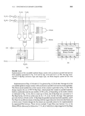
FIGURE 12.23
Implementation of the cascadable up/down binary counter with synchronous parallel load and true
hold capability represented in Fig. 12.22 and by Eqs. (12.6) and (12.7). (a) The Jth stage show-
ing D-to-T flip-flop conversion logic and output logic, (b) Block diagram symbol for the 4-bit
counter.
Implementation of Eqs. (12.6) and (12.7) is given in Fig. 12.23afor the Jth stage of a 4-bit
cascadable up/down binary counter with synchronous parallel load and true hold capability.
The block circuit symbol for a 4-bit version of this counter is provided in Fig. 12.23b. This
design requires the use of FET D flip-flops, which permit the counter to parallel loaded or
hold in a particular state for any number of CK cycles, all depending on the mode controls
as indicated in Fig. 12.22a. But to count up or down, the D flip-flops are converted to T
flip-flops by Eq. (10.10) or, in this case, by Dj = Tj 0 Qj for the Jth stage. This approach
provides the best of both worlds: D flip-flops for parallel load and true hold capability, and T
flip-flops for an efficient means of dealing with the toggle character inherent in the binary up
or down count. Counter designs by this means are especially attractive for implementation
by registered PLD devices. These devices include V-type PALs (see Section 7.4), or the
Xilinx FPGAs discussed in Subsection 7.7.3, all of which have edge-triggered D flip-flops