
Page 612 - Engineering Digital Design
P. 612
582 CHAPTER 12 / MODULE AND BIT-SLICE DEVICES
0 0 Qj True hold _ -
T b b + b p
ab~ i o'j i j
0 1 j Up/down count
1 x ^j Parallel load ( " ^ ^ •* Dj
+
" ' ' " -"S 0 Qj 'ab
(C)
(b)
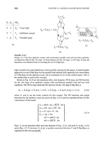
FIGURE 12.22
Design of a 4-bit slice up/down counter with synchronous parallel load and true hold capability.
(a) Operation table for the /th stage, (b) State diagram for the /th stage, (c) NS logic K-map and
minimum cover obtained from (b) assuming the use of D flip-flops.
logic would be too costly (hardware-wise) to justify a design by this means. A much simpler
approach is to use D flip-flops for the parallel load and true hold capability but convert them
to T flip-flops for the up/down count, all on command of two mode-control inputs. This is
the method that is used in this example.
Shown in Fig. 12.22 are the operation table, state diagram, NS K-map, and NS function
for the /th stage of an up/down counter with synchronous parallel load and true hold
capability. The NS K-map yields the NS function for the /th stage D flip-flop as
D J = S lSoQj + S l SoTj+S l P j -+SiS 0Qj + SiS 0(Tj@Qj) + SiPj, (12.6)
where S\ and So are the mode controls for this counter. The NS functions and output
functions for the up/down count are given by Eqs. (12.5) and are reproduced here for the
convenience of the reader:
T A = BCD • Up + BCD • Dn ]
T B = CD-Up + CD- Dn
T c = D • Up + D • Dn
(12.7)
T D= Up + Dn
CO = ABCD • Up
BO = ABCD • Dn
Thus, Tj in the operation table and state diagram of Fig. 12.22, and each Tj in Eq. (12.6)
and in Eqs. (12.7), becomes Tj © Qj to permit conversion between T and D flip-flops, as
explained in the next paragraph.