
Page 616 - Engineering Digital Design
P. 616
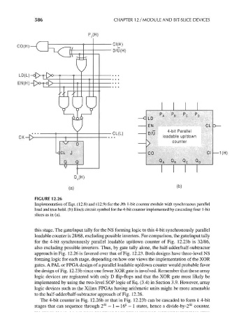
586                              CHAPTER 12 / MODULE AND BIT-SLICE DEVICES


                                          Pj(H)

             CO(H)-/                                CI(H)
                          ~1 < It    "Hi * M. P--'  D/U(H)

                                     r ^ 1
                                     I
                                      V,J
              LD(L)-c|> r{>o-^

              EN(H)_[>o T^>—
                                                    • • •
                                /
                              ' rl '
                                /     /   \
                              \            y"
                                    \ 1 J—                     — C LD  PA   PB   PC   PD
                                    X
                                      ^
                                    \ \.                           EN                     CL
                                    ±               CL(L)          D/g    4-bit Parallel
              CK-0                                                       loadable up/down
                                \s   D                            V         counter
                             <CL J                                CO                      Cl

                                Q    Q                                 QA   Q B Q c   Q 0
                                v

                                    Qj(H)
                                  (a)                                         »)

                    FIGURE 12.26
                    Implementation of Eqs. (12.8) and (12.9) for the /th 1-bit counter module with synchronous parallel
                    load and true hold, (b) Block circuit symbol for the 4-bit counter implemented by cascading four 1-bit
                    slices as in (a).


                    this stage. The gate/input tally for the NS forming logic to this 4-bit synchronously parallel
                    loadable counter is 28/68, excluding possible inverters. For comparison, the gate/input tally
                    for the 4-bit synchronously parallel loadable up/down counter of Fig. 12.23b is 32/86,
                    also excluding possible inverters. Thus, by gate tally alone, the half-adder/half-subtractor
                    approach in Fig. 12.26 is favored over that of Fig. 12.23. Both designs have three-level NS
                    forming logic for each stage, depending on how one views the implementation of the XOR
                    gates. A PAL or FPGA design of a parallel loadable up/down counter would probable favor
                    the design of Fig. 12.23b since one fewer XOR gate is involved. Remember that these array
                    logic devices are registered with only D flip-flops and that the XOR gate must likely be
                    implemented by using the two-level SOP logic of Eq. (3.4) in Section 3.9. However, array
                    logic devices such as the Xilinx FPGAs having arithmetic units might be more amenable
                    to the half-adder/half-subtractor approach of Fig. 12.26.
                       The 4-bit counter in Fig. 12.26b or that in Fig. 12.23b can be cascaded to form k 4-bit
                                                                                    4i
                                                4k
                    stages that can sequence through 2  — 1 = 16* — 1 states, hence a divide-by-2  counter.