
Page 610 - Engineering Digital Design
P. 610
580 CHAPTER 12 / MODULE AND BIT-SLICE DEVICES
h-AH)
-B(H) B(H)
CO(H) — C(H) BO(H) C(H)
L-D(H) D(H)
- Up(H)
P P P P
r
A r B r C r D
LD
Parallel loadable CL >
Up/Down Binary
CO Counter
BO Dn
Q A Q B Q c Q c
•-CL(L) I ' I
Qj(H) (b)
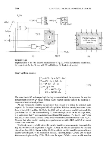
FIGURE 12.20
Implementation of the 4-bit up/down binary counter of Fig. 12.19 with asynchronous parallel load,
(a) Logic circuit for the 7th stage with CO and BO logic, (b) Block circuit symbol.
binary up/down counter:
T A = BCD • Up + BCD • Dn
T c = D • Up + D • Dn
T D= Up + Dn
CO = ABCD • Up
BO = ABCD • Dn
The trend in the NS and output logic having been established, the equations for any size
bidirectional divide-by-2" binary counter can be written directly without the need for K-
maps or minimization algorithms.
All that remains to complete the design of this counter is to obtain the external logic
required for the asynchronous parallel load capability. This has already been done in the
form of Eqs. (12.4) and Fig. 12.10a for the USR with asynchronous parallel load capability
(see Subsection 12.2.4). Presented in Fig. 12.20a is the logic circuit for the jth stage. Here,
it is understood that Tj represents the four different NS functions (T A,T B,T C, and T D) in
Eqs. (12.5) taken in turn, and that LD(L) is the command to parallel load the value Pj(H).
Observe that when parallel loading, the asynchronous overrides PRE and CLR are never
active at the same time.
The block circuit symbol for the 4-bit parallel loadable up/down counter is provided in
Fig. 12.20b. Here, each stage is that of Figure 12.20(a), but with the appropriate NS function
taken from Eqs. (12.5). Shown in Fig. 12.21 is a 4fc-bit parallel loadable up/down binary
counter consisting of k 4-bit counters in cascade. The output logic, CO and BO, for each
4-bit counter is given in Fig. 12.20a. Notice that the input LD(L) is common to all k modules