
Page 727 - Engineering Digital Design
P. 727
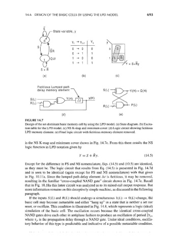
14.6 DESIGN OF THE BASIC CELLS BY USING THE LPD MODEL                693


                                  State variable, y


                                                      Y
                                            0 -> 0
                                            0 -* 1
                                            1 -» 0
                                            1 -» 1


                                                  (b)               (c)

                         Fictitious Lumped path
                         delay memory element \              S(L) —-3 ^\ . y(H) = Q(H)


                                      (d)                             (e)
                 FIGURE 14.7
                 Design of the set-dominant basic memory cell by using the LPD model, (a) State diagram, (b) Excita-
                 tion table for the LPD model, (c) NS K-map and minimum cover, (d) Logic circuit showing fictitious
                 LPD memory element, (e) Final logic circuit with fictitious memory element removed.


                 is the NS K-map and minimum cover shown in Fig. 14.7c. From this there results the NS
                 logic function in LPD notation given by


                                                Y = S + Ry.                         (14.5)
                 Except for the difference in PS and NS nomenclature, Eqs. (14.5) and (10.5) are identical,
                 as they must be. The logic circuit that results from Eq. (14.5) is presented in Fig. 14.7d
                 and is seen to be identical (again except for PS and NS nomenclature) with that given
                 in Fig. 10.1 la. Since the lumped path delay element At is fictitious, it may be removed,
                 resulting in the familiar "cross-coupled NAND gate" circuit shown in Fig. 14.7e. Recall
                 that in Fig. 10.18a this latter circuit was analyzed as to its mixed-rail output response. But
                 more information remains on this deceptively simple machine, as discussed in the following
                 paragraph.
                    If the inputs S(L) and R(L) should undergo a simultaneous 1(L) ->• 0(L) change, the
                 basic cell may become metastable and either "hang up" in a state that is neither a set nor
                 reset, or oscillate. This condition is illustrated in Fig. 14.8, which represents a logic (ideal)
                 simulation of the basic cell. The oscillation occurs because the identical cross-coupled
                 NAND gates drive each other in antiphase fashion to produce an oscillation of period 2r p,
                 where r p is the propagation delay through a NAND gate. Under ideal conditions, oscilla-
                 tory behavior of this type is predictable and indicative of a possible metastable condition.