
Page 728 - Engineering Digital Design
P. 728
694 CHAPTER 14/ASYNCHRONOUS STATE MACHINE DESIGN AND ANALYSIS
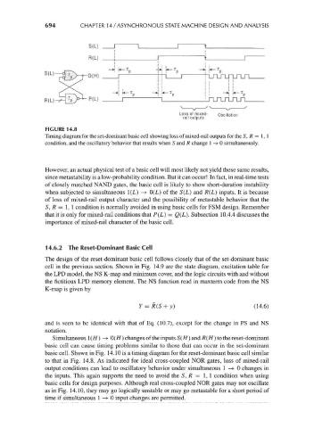
S(L) 1 I 1 '
R(L) i
1 '
— M •+•
Q(H) _l ^J HnJT^r^
I
-*- U-T -* ^— T _^ ^_ T
' P P • P
P(L) 1 n n n n n
Loss of mixed- Oscillation
rail outputs
FIGURE 14.8
Timing diagram for the set-dominant basic cell showing loss of mixed-rail outputs for the 5, R = 1, 1
condition, and the oscillatory behavior that results when S and R change 1—^-0 simultaneously.
However, an actual physical test of a basic cell will most likely not yield these same results,
since metastability is a low-probability condition. But it can occur! In fact, in real-time tests
of closely matched NAND gates, the basic cell is likely to show short-duration instability
when subjected to simultaneous 1(L) -> 0(L) of the S(L) and R(L) inputs. It is because
of loss of mixed-rail output character and the possibility of metastable behavior that the
S, R = 1, 1 condition is normally avoided in using basic cells for FSM design. Remember
that it is only for mixed-rail conditions that P(L) = Q(L). Subsection 10.4.4 discusses the
importance of mixed-rail character of the basic cell.
14.6.2 The Reset-Dominant Basic Cell
The design of the reset-dominant basic cell follows closely that of the set-dominant basic
cell in the previous section. Shown in Fig. 14.9 are the state diagram, excitation table for
the LPD model, the NS K-map and minimum cover, and the logic circuits with and without
the fictitious LPD memory element. The NS function read in maxterm code from the NS
K-map is given by
Y = R(S + y) (14.6)
and is seen to be identical with that of Eq. (10.7), except for the change in PS and NS
notation.
Simultaneous !(//) —>• 0(//) changes of the inputs S(H) and R(H) to the reset-dominant
basic cell can cause timing problems similar to those that can occur in the set-dominant
basic cell. Shown in Fig. 14.10 is a timing diagram for the reset-dominant basic cell similar
to that in Fig. 14.8. As indicated for ideal cross-coupled NOR gates, loss of mixed-rail
output conditions can lead to oscillatory behavior under simultaneous 1 —> 0 changes in
the inputs. This again supports the need to avoid the S, R — 1,1 condition when using
basic cells for design purposes. Although real cross-coupled NOR gates may not oscillate
as in Fig. 14.10, they may go logically unstable or may go metastable for a short period of
time if simultaneous 1 -> 0 input changes are permitted.