
Page 732 - Engineering Digital Design
P. 732
698 CHAPTER 14/ASYNCHRONOUS STATE MACHINE DESIGN AND ANALYSIS
of Fig. 8.46 so as to avoid possible fan-in problems. Recall that propagation delay increases
with increasing number of gate inputs. Notice that a reset-dominant basic cell is used as the
memory element in this case.
14.8 DESIGN OF THE RET D FLIP-FLOP BY USING THE LPD MODEL
The RET D flip-flop was previously designed in Subsection 10.7.2 by using the basic cell
as the memory. In this section the same flip-flop will be designed by using the LPD model.
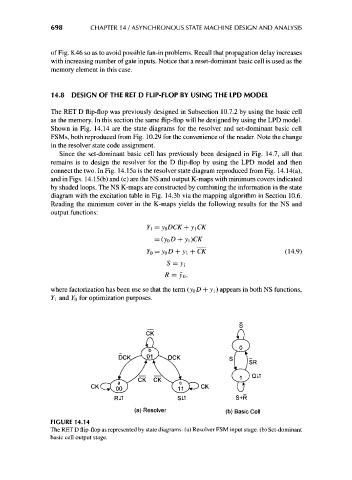
Shown in Fig. 14.14 are the state diagrams for the resolver and set-dominant basic cell
FSMs, both reproduced from Fig. 10.29 for the convenience of the reader. Note the change
in the resolver state code assignment.
Since the set-dominant basic cell has previously been designed in Fig. 14.7, all that
remains is to design the resolver for the D flip-flop by using the LPD model and then
connect the two. In Fig. 14.15a is the resolver state diagram reproduced from Fig. 14.14(a),
and in Figs. 14. 15(b) and (c) are the NS and output K-maps with minimum covers indicated
by shaded loops. The NS K-maps are constructed by combining the information in the state
diagram with the excitation table in Fig. 14. 3b via the mapping algorithm in Section 10.6.
Reading the minimum cover in the K-maps yields the following results for the NS and
output functions:
(14.9)
where factorization has been use so that the term (yoD + y\ ) appears in both NS functions,
Y\ and YQ for optimization purposes.
FW SiT S+R
(a) Resolver (b) Basic Cell
FIGURE 14.14
The RET D flip-flop as represented by state diagrams, (a) Resolver FSM input stage, (b) Set-dominant
basic cell output stage.