
Page 734 - Engineering Digital Design
P. 734
700 CHAPTER 14/ASYNCHRONOUS STATE MACHINE DESIGN AND ANALYSIS
, ., Q(H)
CK(H)-4
D(H)
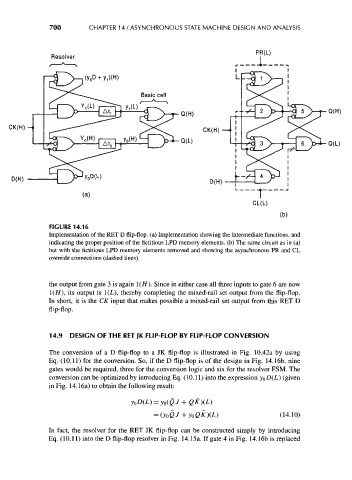
FIGURE 14.16
Implementation of the RET D flip-flop, (a) Implementation showing the intermediate functions, and
indicating the proper position of the fictitious LPD memory elements, (b) The same circuit as in (a)
but with the fictitious LPD memory elements removed and showing the asynchronous PR and CL
override connections (dashed lines).
the output from gate 3 is again !(//). Since in either case all three inputs to gate 6 are now
!(//), its output is 1(L), thereby completing the mixed-rail set output from the flip-flop.
In short, it is the CK input that makes possible a mixed-rail set output from this RET D
flip-flop.
1 4.9 DESIGN OF THE RET JK FLIP-FLOP BY FLIP-FLOP CONVERSION
The conversion of a D flip-flop to a JK flip-flop is illustrated in Fig. 10.42a by using
Eq. (10.11) for the conversion. So, if the D flip-flop is of the design in Fig. 14.16b, nine
gates would be required, three for the conversion logic and six for the resolver FSM. The
conversion can be optimized by introducing Eq. (10.1 1) into the expression yoD(L) (given
in Fig. 14.16a) to obtain the following result:
(14.10)
In fact, the resolver for the RET JK flip-flop can be constructed simply by introducing
Eq. (10.11) into the D flip-flop resolver in Fig. 14.15a. If gate 4 in Fig. 14.16b is replaced