Page 729 - Engineering Digital Design
P. 729

14.7 DESIGN OF THE RENDEZVOUS MODULES                                695
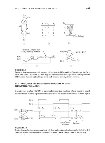


                                            y«        Y

                                                       0
                                            0 -> 1     1
                                            1 -» o     0
                                            1 -» 1                    \^   Y = R(S+y)


                                                  (b)                (c)


                         Fictitious Lumped path
                         delay memory element \              R(H)-^ V-f- Y(H) = Q(H)


                                      (d)                             (e)
                 FIGURE 14.9
                 Design of the reset-dominant basic memory cell by using the LPD model, (a) State diagram, (b) Exci-
                 tation table for the LPD model, (c) NS K-map and minimum cover, (d) Logic circuit showing fictitious
                 LPD memory element, (e) Final logic circuit with fictitious memory element removed.


                 14.7 DESIGN OF THE RENDEZVOUS MODULES BY USING
                 THE NESTED CELL MODEL

                 A rendezvous module (RMOD) is an asynchronous state machine whose output is issued
                 active when all external inputs become active and is issued inactive when all external inputs


                               S(H)

                               R(H)                                 1            1
                                         .   l        -^  L T      _^. ;  _
                                         r*~ p          i*  p       * :"*" P
                                        _J                            n n n n n
                                         I :
                                                                      •     ^ j T
                                        "*i *~ p    ~*  ^^ P          :         P

                                                             Loss of mixed-  Oscillation
                                                              rail outputs
                 FIGURE 14.10
                 Timing diagram for the reset-dominant basic cell showing loss of mixed-rail outputs for the S, /? = 1, 1
                 condition, and the oscillatory behavior that results when S and R change 1 —»• 0 simultaneously.
   724   725   726   727   728   729   730   731   732   733   734