
Page 731 - Engineering Digital Design
P. 731
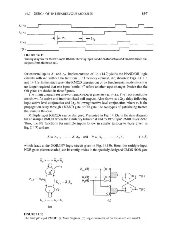
14.7  DESIGN OF THE RENDEZVOUS MODULES                               697


              A,(H)

              A 0(H)


              Y(H)
               Y(L)
                 FIGURE 14.12
                 Timing diagram for the two-input RMOD showing input conditions for active and inactive mixed-rail
                 outputs from the basic cell.


                 for external inputs A\ and A 0. Implementation of Eq. (14.7) yields the NAND/OR logic
                 circuits with and without the fictitious LPD memory element, Af, shown in Figs. 14.lid
                 and 14.1 le. In the strict sense, the RMOD operates out of the fundamental mode since it is
                 no longer required that one input "settle in" before another input changes. Notice that the
                 OR gates are shaded in these figures.
                   The timing diagram for the two-input RMOD is given in Fig. 14.12. The input conditions
                 are shown for active and inactive mixed-rail outputs. Also shown is a 2r p delay following
                 input active level conjunction and 3r p following inactive level conjunction, where T P is the
                 propagation delay through a NAND gate or OR gate, the two types of gates being treated
                 the same in this case.
                   Multiple input RMODs can be designed. Presented in Fig. 14.13a is the state diagram
                 for an n-input RMOD where the similarity between it and the two-input RMOD is evident.
                 Thus, the NS functions for multiple inputs follow in similar fashion to those given in
                 Eq. (14.7) and are

                               S = A W _,    A,A 0 and R = A n-i       AjA ,        (14.8)

                 which leads to the NOR/INV logic circuit given in Fig. 14.13b. Here, the multiple-input
                 NOR gates (shown shaded) can be configured as in the specially designed CMOS NOR gate


                         A    +  +A  +A
                          n-1 -"   1  0


                   A   ... A A /  \               AjOH)
                   M     M M
                    n-1   1 0      _              A (\-i\
                                                    H
                                   A n ,-AA       A o< >
                                   YiT                           j ^U^l H^Y(H)

                         A    +  +                              (b)
                           n-i - VA 0
                              (a)
                 FIGURE 14.13
                 The multiple input RMOD. (a) State diagram, (b) Logic circuit based on the nested cell model.