
Page 733 - Engineering Digital Design
P. 733
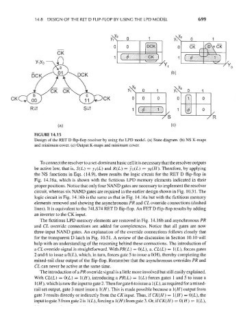
14.8 DESIGN OF THE RET D FLIP-FLOP BY USING THE LPD MODEL            699


                           (a)                                            (c)
                  FIGURE 14.15
                  Design of the RET D flip-flop resolver by using the LPD model, (a) State diagram, (b) NS K-maps
                  and minimum cover, (c) Output K-maps and minimum cover.


                    To connect the resolver to a set-dominant basic cell it is necessary that the resolver outputs
                  be active low, that is, S(L) = y\(L} and R(L) = yo(L) = yo(H). Therefore, by applying
                  the NS functions in Eqs. (14.9), there results the logic circuit for the RET D flip-flop in
                  Fig. 14.16a, which is shown with the fictitious LPD memory elements indicated in their
                  proper positions. Notice that only four NAND gates are necessary to implement the resolver
                  circuit, whereas six NAND gates are required in the earlier design shown in Fig. 10.31. The
                  logic circuit in Fig. 14.16b is the same as that in Fig. 14.16a but with the fictitious memory
                  elements removed and showing the asynchronous PR and CL override connections (dashed
                  lines). It is equivalent to the 74LS74 RET D flip-flop. An FET D flip-flop results by adding
                  an inverter to the CK input.
                    The fictitious LPD memory elements are removed in Fig. 14.16b and asynchronous PR
                  and CL override connections are added for completeness. Notice that all gates are now
                  three-input NAND gates. An explanation of the override connections follows closely that
                  for the transparent D latch in Fig. 10.51. A review of the discussion in Section 10.10 will
                  help with an understanding of the reasoning behind these connections. The introduction of
                  a CL override signal is straightforward. With PR(L) = 0(L), a, CL(L) = 1(L), forces gates
                  2 and 6 to issue a 0(L), which, in turn, forces gate 5 to issue a 0(H), thereby completing the
                  mixed-rail clear output of the flip-flop. Remember that the asynchronous overrides PR and
                  CL can never be active at the same time.
                    The introduction of a PR override signal is a little more involved but still easily explained.
                  With CL(L) = 0(L) = 1(H), introducing a PR(L) = 1(L) forces gates 1 and 5 to issue a
                  !(//), which is now the input to gate 2. Then for gate 6 to issue a 1 (L), as required for a mixed-
                  rail set output, gate 3 must issue a !(//). This is made possible because a !(//) output from
                  gate 3 results directly or indirectly from the CK input. Thus, if CK(H) = l(H ) = 0(L), the
                  input to gate 3 from gate 2 is 1(L), forcing a l(H ) from gate 3. Or, if CK(H} = Q(H) = 1(L),