Page 270 - System on Package_ Miniaturization of the Entire System
P. 270

244    Cha pte r  F o u r


                    calculation, a dielectric loss of tan d = 0.02 and a copper conductivity of σ = 5.8 × 10 7
                                                                                   c
                    siemens per meter (S/m) were used. The stopband predicted with Figure 4.95a is
                    superposed on Figure 4.95b. This figure indicates that the stopband predicted from the
                    dispersion diagram has good agreement with the measured and simulated data.

                    Two-Dimensional Unit-Cell Analysis
                    If the unit cells are connected with each other to form a 2D lattice, the 1D dispersion
                    diagram analysis becomes inaccurate, since wave propagation can be possible in any
                    direction on the plane in a 2D EBG, as opposed to the linear wave propagation in a 1D
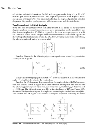
                    EBG structure. Hence, the 1D analysis needs to be extended for 2D structures. Figure 4.96
                    shows the port definitions for a 1D and 2D EBG. Now, focusing on the x and y directions,
                    the following network matrix becomes useful:

                                                  ⎛ V ⎞   ⎛ V ⎞
                                                  ⎜  1 ⎟  ⎜  I −  3  ⎟
                                                  ⎜  I 1 ⎟  =  F ⎜  3 ⎟
                                                  ⎜ V ⎟   ⎜ V ⎟                         (4.36)
                                                  ⎜  2 ⎟  ⎜  4  ⎟ ⎟
                                                    I ⎝  2 ⎠  ⎝  I − ⎠
                                                             4
                       Based on this matrix, the following eigenvalue equation can be used to generate the
                    2D dispersion diagram:

                                        ⎧    e ⎛  γ xx d       ⎞ ⎫ ⎫  ⎞
                                        ⎪   ⎜                  ⎟  ⎪ ⎛ V 3  ⎟
                                                                 ⎜
                                        ⎪   ⎜     e γ xx d     ⎟ ⎪ −I  ⎟
                                                                 ⎜
                                        ⎨ F −  ⎜        γ      ⎟  ⎬  3  = 0             (4.37)
                                        ⎪   ⎜          e  yy d  ⎟ ⎪ ⎜ V 4  ⎟ ⎟
                                                                 ⎜
                                        ⎪   ⎜                γ yy d ⎟ ⎪ − ⎠
                                                                 ⎝ I
                                        ⎩   ⎝               e  ⎠  ⎭  4
                                                         −γ xx d
                       In this equation the propagation factor  e   is for the interval d  in the +x direction
                                                                             x
                         −γ yy d
                    and e    is for the interval d  in the +y direction.
                                            y
                       Based on the 2D dispersion diagram analysis, the stopband of the 2D EBG structure
                    with slits (case b) shown in Figure 4.97a and b has been investigated. The unit cell has
                    the following parameters: w = 0.25 mm, w = 14.73 mm, w = 0.13 mm, g = 0.25 mm, and
                                                       2
                                                                               1
                                           1
                                                                    3
                    g = 7.62 mm. The dielectric used was FR4 with a thickness of 127 μm. Figure 4.97c
                     2
                    shows the 2D dispersion diagram that is plotted accounting for the Brillouin zone [94a].
                    The colored area of Figure 4.97c shows a complete stopband indicating no wave
                                                                     V 4
                                                                  I 4
                                  I in              I out    I 1              I 3
                                        Z 11  Z 12                 Z 11  Z 12
                               V in                  V out  V 1                 V 3
                                        Z 21  Z 22                 Z 21  Z 22
                                    y                      y
                                                                  I
                                        x                      x  2
                                                                      V 2
                    FIGURE 4.96  Network representation—two port (left) and four port (right).
   265   266   267   268   269   270   271   272   273   274   275