
Page 274 - System on Package_ Miniaturization of the Entire System
P. 274
248 Cha pte r F o u r
4.8.3 Radiation Analysis of EBGs
The AI-EBG structure has periodic gaps that can radiate energy if the AI-EBG structure
is used as a reference plane. This is because return currents are forced to flow around
the splits, and charges therefore accumulate on their edges [95], which create a source
of far field radiation [96]. Hence, the splits or gaps in a reference plane can be considered
as slot antennas that can interfere with other devices. This causes an electromagnetic
interference (EMI) problem. In this section, near-field and far-field analysis for three
test vehicles are shown through simulations and measurements to better understand
the radiation mechanisms of the AI-EBG structure.
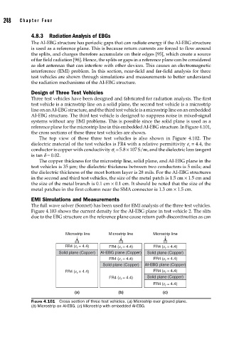
Design of Three Test Vehicles
Three test vehicles have been designed and fabricated for radiation analysis. The first
test vehicle is a microstrip line on a solid plane, the second test vehicle is a microstrip
line on an AI-EBG structure, and the third test vehicle is a microstrip line on an embedded
AI-EBG structure. The third test vehicle is designed to suppress noise in mixed-signal
systems without any EMI problems. This is possible since the solid plane is used as a
reference plane for the microstrip line in this embedded AI-EBG structure. In Figure 4.101,
the cross sections of these three test vehicles are shown.
The top view of these three test vehicles is also shown in Figure 4.102. The
dielectric material of the test vehicles is FR4 with a relative permittivity e = 4.4, the
r
conductor is copper with conductivity s = 5.8 × 10⁷ S/m, and the dielectric loss tangent
c
is tan d = 0.02.
The copper thickness for the microstrip line, solid plane, and AI-EBG plane in the
test vehicles is 35 μm; the dielectric thickness between two conductors is 5 mils; and
the dielectric thickness of the most bottom layer is 28 mils. For the AI-EBG structures
in the second and third test vehicles, the size of the metal patch is 1.5 cm × 1.5 cm and
the size of the metal branch is 0.1 cm × 0.1 cm. It should be noted that the size of the
metal patches in the first column near the SMA connector is 1.3 cm × 1.5 cm.
EMI Simulations and Measurements
The full wave solver (Sonnet) has been used for EMI analysis of the three test vehicles.
Figure 4.103 shows the current density for the AI-EBG plane in test vehicle 2. The slits
due to the EBG structure on the reference plane cause return path discontinuities as can
Microstrip line Microstrip line Microstrip line
FR4 (e = 4.4) FR4 (e r = 4.4) FR4 (e r = 4.4)
r
Solid plane (Copper) AI-EBG plane (Copper) Solid plane (Copper)
FR4 (e = 4.4) FR4 (e = 4.4)
r
r
Solid plane (Copper) AI-EBG plane (Copper)
FR4 (e = 4.4) FR4 (e = 4.4)
r
r
FR4 (e = 4.4) Solid plane (Copper)
r
FR4 (e r = 4.4)
(a) (b) (c)
FIGURE 4.101 Cross section of three test vehicles. (a) Microstrip over ground plane.
(b) Microstrip on AI-EBG. (c) Microstrip with embedded AI-EBG.