
Page 75 - System on Package_ Miniaturization of the Entire System
P. 75
52 Cha pte r T w o
While it’s desirable, from a design cycle time perspective, to have all the IPs available
before the start of the SOC create process, in many cases, the IPs are developed
concurrently with the chip. This helps reduce the overall cycle time but makes it critically
important for the chip create team to work closely with the IP team, to ensure that the
IP is developed to meet the chip requirements.
For SOCs that aggressively adopt the new process technologies, the chip design
starts even before the manufacturing process is completely qualified and the transistor
and interconnect characteristics are stabilized. The design team hence needs to work
closely with the silicon technology development team to be able to adapt quickly to
process changes. This concurrent engineering can also be leveraged to tune the
manufacturing process so as to meet a critical SOC requirement such as leakage power
and/or performance.
The package is a key contributor to the cost, performance, power dissipation, and
form factor of an SOC. It is hence becoming increasingly important to do package design
concurrently with SOC design.
In the following sections we discuss two examples of these concurrent engineering
challenges in further detail.
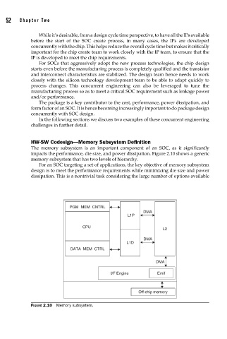
HW-SW Codesign—Memory Subsystem Definition
The memory subsystem is an important component of an SOC, as it significantly
impacts the performance, die size, and power dissipation. Figure 2.10 shows a generic
memory subsystem that has two levels of hierarchy.
For an SOC targeting a set of applications, the key objective of memory subsystem
design is to meet the performance requirements while minimizing die size and power
dissipation. This is a nontrivial task considering the large number of options available
PGM MEM CNTRL
DMA
L1P
CPU
L2
DMA
L1D
DATA MEM CTRL
DMA
I/F Engine Emif
Off-chip memory
FIGURE 2.10 Memory subsystem.