
Page 79 - System on Package_ Miniaturization of the Entire System
P. 79
56 Cha pte r T w o
A E
D
C
B F
(a)
(b)
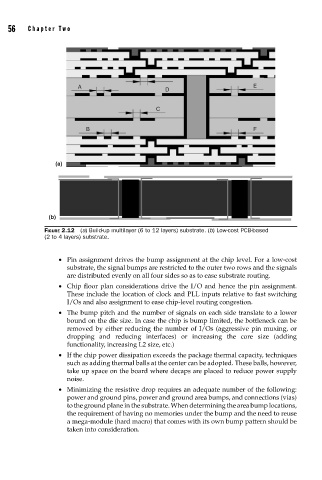
FIGURE 2.12 (a) Build-up multilayer (6 to 12 layers) substrate. (b) Low-cost PCB-based
(2 to 4 layers) substrate.
• Pin assignment drives the bump assignment at the chip level. For a low-cost
substrate, the signal bumps are restricted to the outer two rows and the signals
are distributed evenly on all four sides so as to ease substrate routing.
• Chip floor plan considerations drive the I/O and hence the pin assignment.
These include the location of clock and PLL inputs relative to fast switching
I/Os and also assignment to ease chip-level routing congestion.
• The bump pitch and the number of signals on each side translate to a lower
bound on the die size. In case the chip is bump limited, the bottleneck can be
removed by either reducing the number of I/Os (aggressive pin muxing, or
dropping and reducing interfaces) or increasing the core size (adding
functionality, increasing L2 size, etc.)
• If the chip power dissipation exceeds the package thermal capacity, techniques
such as adding thermal balls at the center can be adopted. These balls, however,
take up space on the board where decaps are placed to reduce power supply
noise.
• Minimizing the resistive drop requires an adequate number of the following:
power and ground pins, power and ground area bumps, and connections (vias)
to the ground plane in the substrate. When determining the area bump locations,
the requirement of having no memories under the bump and the need to reuse
a mega-module (hard macro) that comes with its own bump pattern should be
taken into consideration.