Page 78 - System on Package_ Miniaturization of the Entire System
P. 78

Intr oduction to System-on-Chip (SOC)     55


                                          Stitch pads                      Mold
                                                        Solder mask
                             Copper pad                                            Die


                                                                                       Epoxy


                                      Solder connection  Polymide               Dummy pads
                      (a)

                                                   Lid/mold compound


                        Lid attach                                                Die
                         epoxy
                                                                                  Underfill


                                                                                  Substrate


                                                         BGA
                        (b)

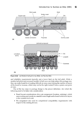
                    FIGURE 2.11  (a) Wirebond ball grid array (BGA). (b) Flip-chip BGA.
                    and reliability requirements typically put a lower limit on the ball pitch. While a
                    smaller ball pitch and increased number of ball rows can help reduce the package size,
                    they can make board-level routing difficult, in some cases forcing the number of layers
                    of the board to increase, which may not be the right tradeoff from a system cost point
                    of view.
                       One of the key steps in package design is the pinout definition—for which the
                    following need to be taken into consideration:
                        •  Board layout considerations drive pin assignment (location, ordering), which
                           eases routing and results in a smaller route length and a board with fewer layers
                           (a low system-level cost).
                        •  Pin assignment also need to comprehend compatibility requirements with
                           respect to the existing devices.
   73   74   75   76   77   78   79   80   81   82   83