
Page 264 -
P. 264
LIGA and Micromolding 4-5
remains an elusive goal. In LIGA, mold inserts are made via X-ray lithography, but depending on the
dimensions of the micro parts, the accuracy requirements, and the fabrication costs, mold inserts may
also be realized by e-beam writing, computer numerically controlled (CNC) machining, wet Si bulk
micromachining, deep UV resists, deep reactive ion etching (DRIE), ultrasonic cutting, excimer laser
ablation, electrodischarge machining (EDM), and laser cutting (see Figure 4.2).
4.2.2 Synchrotron Orbital Radiation (SOR)
4.2.2.1 Introduction
Lithography based on synchrotron radiation, also called synchrotron orbital radiation (SOR), is prima-
rily pursued with the aim of adopting the technology as an industrial tool for the large-scale manufacture
of microelectronic circuits with characteristic dimensions in the submicron range [Waldo and Yanof,
1991; Hill, 1991]. Synchrotron radiation sources “outshine” electron impact and plasma sources for
generating X-rays. They emit a much higher flux of usable collimated X-rays, thereby allowing shorter
exposure times and larger throughputs. The pros and cons of X-ray radiation for lithography in IC
manufacture are summarized in Table 4.1.
Despite the many promising features of X-ray lithography, the technique still lacks mainstream accept-
ance in the IC industry. In 1991, experts projected that X-ray lithography would be in use by 1995 for
64-Mb DRAM manufacture, with critical dimensions (CDs) around 0.3 to 0.4µm. With more certainty,
they projected that the transition to X-rays would occur with the 0.2 to 0.3 µm CDs of 256-Mb DRAMs
by 1998 [Waldo and Yanof, 1991]. Both dates passed without the emergence of the industrial use of
X-rays. Continued improvements in optical lithography outpace the industrial use of X-ray lithography
for IC applications. However, its use for prototype development on a small scale will no doubt continue.
In addition to being an option for next-generation IC lithography, X-rays are also used in the fabrica-
tion of 3-D microstructures. In LIGA, synchrotron radiation is used only in the lithography step. Other
micromachining applications for SOR do exist. Urisu and his colleagues, for example, explored the use of
synchrotron radiation for radiation-excited chemical vapor deposition and etching [Urisu and Kyuragi,
1987]. Micromachinists are hoping to piggyback X-ray lithography research and development efforts for
the fabrication of micromachines onto major IC projects. The use of X-ray lithography for fabricating
micro devices other than integrated circuits does not yet present a large business opportunity by itself.
Not having a major IC product line associated with X-ray lithography makes it difficult to justify the use
of X-ray lithography for micromachining, especially since other, less expensive micromachining tech-
nologies have not yet opened up the type of mass markets expected in the IC world. The fact that the
X-rays used in LIGA are shorter in wavelength than in the IC application (2 to 10Å vs. 20 to 50Å) also puts
micromachinists at a disadvantage. For example, the soft X-rays in the IC industry may eventually be gen-
erated from a much less expensive source,such as a transition radiation source [Goedtkindt et al.,1991].Also,
nontraditional IC materials are frequently employed in LIGA. The fabrication of X-ray masks poses more
difficulties than masks for IC applications. Rotation and slanting of the X-ray masks to craft nonvertical
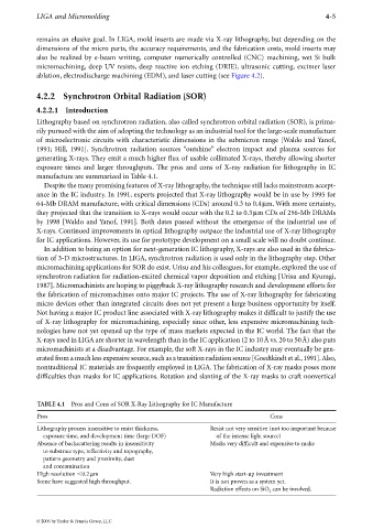
TABLE 4.1 Pros and Cons of SOR X-Ray Lithography for IC Manufacture
Pros Cons
Lithography process insensitive to resist thickness, Resist not very sensitive (not too important because
exposure time, and development time (large DOF) of the intense light source)
Absence of backscattering results in insensitivity Masks very difficult and expensive to make
to substrate type, reflectivity and topography,
pattern geometry and proximity, dust
and contamination
High resolution 0.2µm Very high start-up investment
Some have suggested high throughput. It is not proven as a system yet.
Radiation effects on SiO can be involved.
2
© 2006 by Taylor & Francis Group, LLC