
Page 454 - Organic Electronics in Sensors and Biotechnology
P. 454
Light (top)
x
S D
Au Au
t
d
C 60 + ZnPc
Interface BCB
x = 0
ITO
G G
Light (bottom)
10 –5
10 –6
10 –5
2.2 mW; through ITO
10 –7 2.9 mW; through ITO
3.7 mW; through ITO
3.7 mW; through Au
I d (A) 10 –8 Drain current (A) 10 –6 2.9 mW; through Au
2.2 mW; through
Au
2.9 mW; 780 nm
10 –9 λ = 780 nm 2.2 mW; 780 nm
–60 –30 0 30 60 3.7 mW; 780 nm
Gate voltage (V) Dark
10 –10 21 μW; 530 nm
66 μW; 530 nm
110 μW; 530 nm
10 –11
–60 –40 –20 0 20 40 60
V (V)
g
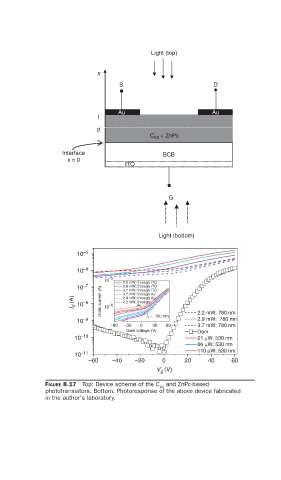
FIGURE 8.17 Top: Device scheme of the C and ZnPc-based
60
phototransistors. Bottom: Photoresponse of the above device fabricated
in the author’s laboratory.