
Page 238 - Power Electronic Control in Electrical Systems
P. 238
//SYS21/F:/PEC/REVISES_10-11-01/075065126-CH006.3D ± 226 ± [177±262/86] 17.11.2001 10:23AM
226 Power electronic equipment
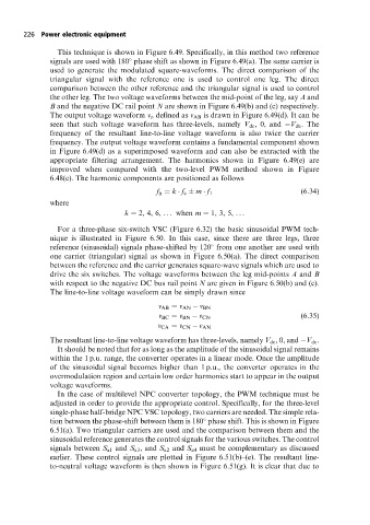
This technique is shown in Figure 6.49. Specifically, in this method two reference
signals are used with 180 phase shift as shown in Figure 6.49(a). The same carrier is
used to generate the modulated square-waveforms. The direct comparison of the
triangular signal with the reference one is used to control one leg. The direct
comparison between the other reference and the triangular signal is used to control
the other leg. The two voltage waveforms between the mid-point of the leg, say A and
B and the negative DC rail point N are shown in Figure 6.49(b) and (c) respectively.
The output voltage waveform v o defined as v AB is drawn in Figure 6.49(d). It can be
seen that such voltage waveform has three-levels, namely V dc , 0, and V dc . The
frequency of the resultant line-to-line voltage waveform is also twice the carrier
frequency. The output voltage waveform contains a fundamental component shown
in Figure 6.49(d) as a superimposed waveform and can also be extracted with the
appropriate filtering arrangement. The harmonics shown in Figure 6.49(e) are
improved when compared with the two-level PWM method shown in Figure
6.48(c). The harmonic components are positioned as follows
f h k f c m f 1 (6:34)
where
k 2, 4, 6, ... when m 1, 3, 5, ...
For a three-phase six-switch VSC (Figure 6.32) the basic sinusoidal PWM tech-
nique is illustrated in Figure 6.50. In this case, since there are three legs, three
reference (sinusoidal) signals phase-shifted by 120 from one another are used with
one carrier (triangular) signal as shown in Figure 6.50(a). The direct comparison
between the reference and the carrier generates square-wave signals which are used to
drive the six switches. The voltage waveforms between the leg mid-points A and B
with respect to the negative DC bus rail point N are given in Figure 6.50(b) and (c).
The line-to-line voltage waveform can be simply drawn since
v AB v AN v BN
v BC v BN v CN (6:35)
v CA v CN v AN
The resultant line-to-line voltage waveform has three-levels, namely V dc , 0, and V dc .
It should be noted that for as long as the amplitude of the sinusoidal signal remains
within the 1 p.u. range, the converter operates in a linear mode. Once the amplitude
of the sinusoidal signal becomes higher than 1 p.u., the converter operates in the
overmodulation region and certain low order harmonics start to appear in the output
voltage waveforms.
In the case of multilevel NPC converter topology, the PWM technique must be
adjusted in order to provide the appropriate control. Specifically, for the three-level
single-phase half-bridge NPC VSC topology, two carriers are needed. The simple rela-
tion between the phase-shift between them is 180 phase shift. This is shown in Figure
6.51(a). Two triangular carriers are used and the comparison between them and the
sinusoidal reference generates the control signals for the various switches. The control
signals between S a1 and S a3 , and S a2 and S a4 must be complementary as discussed
earlier. These control signals are plotted in Figure 6.51(b)±(e). The resultant line-
to-neutral voltage waveform is then shown in Figure 6.51(g). It is clear that due to