Page 766 - Engineering Digital Design
P. 766
732         CHAPTER 14/ASYNCHRONOUS STATE MACHINE DESIGN AND ANALYSIS


                    generated during several of the transitions. With this in mind, the results are given collec-
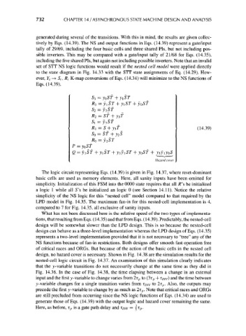
                    tively by Eqs. (14.39). The NS and output functions in Eqs. (14.39) represent a gate/input
                    tally of 29/69, including the four basic cells and three shared Pis, but not including pos-
                    sible inverters. This may be compared with a gate/input tally of 21/68 for Eqs. (14.35),
                    including the five shared Pis, but again not including possible inverters. Note that an invalid
                    set of STT NS logic functions would result if the nested cell model were applied directly
                    to the state diagram in Fig. 14.33 with the STT state assignments of Eq. (14.29). How-
                    ever, Yi —> Sf, Rj K-map conversions of Eqs. (14.34) will minimize to the NS functions of
                    Eqs. (14.39).


                                           S 3=y QSf+yiST

                                           S 2 = yiS f
                                           R 2 = ST +y 3f


                                                                                      (14.39)
                                           So = '
                                           *o =
                                   P=y 0 Sf
                                                              y 0ST
                                                                     Hazard cover

                       The logic circuit representing Eqs. (14.39) is given in Fig. 14.37, where reset-dominant
                    basic cells are used as memory elements. Here, all sanity inputs have been omitted for
                    simplicity. Initialization of this FSM into the 0000 state requires that all R's be initialized
                    a logic 1 while all S's be initialized an logic 0 (see Section 14.11). Notice the relative
                    simplicity of the NS logic for this "nested cell" model compared to that required by the
                    LPD model in Fig. 14.35. The maximum fan-in for this nested-cell implementation is 4,
                    compared to 7 for Fig. 14.35, all exclusive of sanity inputs.
                      What has not been discussed here is the relative speed of the two types of implementa-
                    tions, that resulting from Eqs. (14.35) and that from Eqs. (14.39). Predictably, the nested-cell
                    design will be somewhat slower than the LPD design. This is so because the nested-cell
                    design can behave as a three-level implementation whereas the LPD design of Eqs. (14.35)
                    represents a two-level implementation provided that it is not necessary to "tree" any of the
                    NS functions because of fan-in restrictions. Both designs offer smooth fast operation free
                    of critical races and ORGs. But because of the action of the basic cells in the nested cell
                    design, no hazard cover is necessary. Shown in Fig. 14.38 are the simulation results for the
                    nested-cell logic circuit in Fig. 14.37. An examination of this simulation clearly indicates
                    that the y-variable transitions do not necessarily change at the same time as they did in
                    Fig. 14.36. In the case of Fig. 14.38, the time elapsing between a change in an external
                    input and the first y-variable to change varies from 2x p to (3r p + T///V) and the time between
                    y-variable changes for a single transition varies from r^v to 2r p. Also, the outputs may
                    precede the first y-variable to change by as much as 2r p. Note that critical races and ORGs
                    are still precluded from occurring since the NS logic functions of Eqs. (14.34) are used to
                    generate those of Eqs. (14.39) with the output logic and hazard cover remaining the same.
                    Here, as before, T P is a gate path delay and

