
Page 192 - Mechatronic Systems Modelling and Simulation with HDLs
P. 192
8.2 DEMONSTRATOR 5: CAPACITIVE PRESSURE SENSOR 181
are each depicted by the small triangles. The scatter between the measurements is
caused by the scatter between the circuits. The simulation reflects the measured
trace with an accuracy of below 10%. It also shows that the simulation remains a
little behind the measurements at higher pressures and thus greater deflections. This
effect could be caused by the stronger electrostatic forces of the read-out voltage
at greater deflections, which are not taken into account in the model. Overall, this
type of simulation permits the investigation of the overall function of the system,
and also its sensitivity and linearity. This is accomplished even before manufacture.
For the case shown, such a system simulation requires around 77 CPU minutes on
a SUN Sparc 20.
Parametric simulations
In a circuit simulator it is normal to vary the models based upon parameters, in
order to cover as broad an application spectrum as possible. Such parameters can
be yielded from the geometry of the structure and from the material properties.
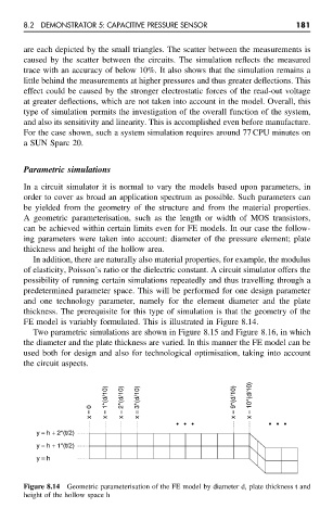
A geometric parameterisation, such as the length or width of MOS transistors,
can be achieved within certain limits even for FE models. In our case the follow-
ing parameters were taken into account: diameter of the pressure element; plate
thickness and height of the hollow area.
In addition, there are naturally also material properties, for example, the modulus
of elasticity, Poisson’s ratio or the dielectric constant. A circuit simulator offers the
possibility of running certain simulations repeatedly and thus travelling through a
predetermined parameter space. This will be performed for one design parameter
and one technology parameter, namely for the element diameter and the plate
thickness. The prerequisite for this type of simulation is that the geometry of the
FE model is variably formulated. This is illustrated in Figure 8.14.
Two parametric simulations are shown in Figure 8.15 and Figure 8.16, in which
the diameter and the plate thickness are varied. In this manner the FE model can be
used both for design and also for technological optimisation, taking into account
the circuit aspects.
x = 1*(d/10) x = 2*(d/10) x = 3*(d/10) x = 9*(d/10) x = 10*(d/10)
x = 0
• • • • • •
y = h + 2*(t/2)
y = h + 1*(t/2)
y = h
Figure 8.14 Geometric parameterisation of the FE model by diameter d, plate thickness t and
height of the hollow space h