
Page 208 - Rashid, Power Electronics Handbook
P. 208
12 Three-Phase Controlled Recti®ers 197
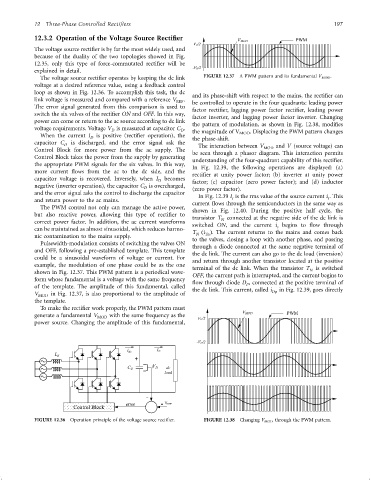
12.3.2 Operation of the Voltage Source Rectifier
V MOD
V D/2
The voltage source recti®er is by far the most widely used, and
because of the duality of the two topologies showed in Fig.
12.35, only this type of force-commutated recti®er will be
explained in detail.
The voltage source recti®er operates by keeping the dc link FIGURE 12.37 A PWM pattern and its fundamental V MOD .
voltage at a desired reference value, using a feedback control
loop as shown in Fig. 12.36. To accomplish this task, the dc and its phase-shift with respect to the mains, the recti®er can
link voltage is measured and compared with a reference V REF . be controlled to operate in the four quadrants: leading power
The error signal generated from this comparison is used to
factor recti®er, lagging power factor recti®er, leading power
switch the six valves of the recti®er ON and OFF. In this way,
factor inverter, and lagging power factor inverter. Changing
power can come or return to the ac source according to dc link
the pattern of modulation, as shown in Fig. 12.38, modi®es
voltage requirements. Voltage V is measured at capacitor C .
D D the magnitude of V MOD . Displacing the PWM pattern changes
When the current I is positive (recti®er operation), the
D the phase-shift.
capacitor C is discharged, and the error signal ask the
D The interaction between V and V (source voltage) can
MOD
Control Block for more power from the ac supply. The be seen through a phasor diagram. This interaction permits
Control Block takes the power from the supply by generating
understanding of the four-quadrant capability of this recti®er.
the appropriate PWM signals for the six valves. In this way,
In Fig. 12.39, the following operations are displayed: (a)
more current ¯ows from the ac to the dc side, and the
recti®er at unity power factor; (b) inverter at unity power
capacitor voltage is recovered. Inversely, when I D becomes factor; (c) capacitor (zero power factor); and (d) inductor
negative (inverter operation), the capacitor C is overcharged, (zero power factor).
D
and the error signal asks the control to discharge the capacitor
In Fig. 12.39 I is the rms value of the source current i . This
s
s
and return power to the ac mains.
current ¯ows through the semiconductors in the same way as
The PWM control not only can manage the active power,
shown in Fig. 12.40. During the positive half cycle, the
but also reactive power, allowing this type of recti®er to
transistor T connected at the negative side of the dc link is
N
correct power factor. In addition, the ac current waveforms
switched ON, and the current i begins to ¯ow through
s
can be maintained as almost sinusoidal, which reduces harmo-
T ði Þ. The current returns to the mains and comes back
N
Tn
nic contamination to the mains supply.
to the valves, closing a loop with another phase, and passing
Pulsewidth-modulation consists of switching the valves ON through a diode connected at the same negative terminal of
and OFF, following a pre-established template. This template the dc link. The current can also go to the dc load (inversion)
could be a sinusoidal waveform of voltage or current. For and return through another transistor located at the positive
example, the modulation of one phase could be as the one
terminal of the dc link. When the transistor T N is switched
shown in Fig. 12.37. This PWM pattern is a periodical wave-
OFF, the current path is interrupted, and the current begins to
form whose fundamental is a voltage with the same frequency
¯ow through diode D , connected at the positive terminal of
P
of the template. The amplitude of this fundamental, called
the dc link. This current, called i Dp in Fig. 12.39, goes directly
V in Fig. 12.37, is also proportional to the amplitude of
MOD
the template.
To make the recti®er work properly, the PWM pattern must
generate a fundamental V MOD with the same frequency as the V D/2 V MOD
power source. Changing the amplitude of this fundamental,
-V D/2
L S
FIGURE 12.36 Operation principle of the voltage source recti®er. FIGURE 12.38 Changing V MOD through the PWM pattern.