
Page 211 - Rashid, Power Electronics Handbook
P. 211
200 J. W. Dixon
where DP ðSÞ and DP ðSÞ represent the input and output +
1
2
power of the recti®er in Laplace dominion, V the rms value of I_ref D Q PWM
the mains voltage supply (phase-to-neutral), I the input (a) - flip-flop
S
current being controlled by the template, L the input induc- sampling clock
S
tance, and R the resistance between the converter and power CLK
supply. According to stability criteria, and assuming a PI
controller, the following relations are obtained:
hysteresis band adjust
C V D
D
I ð12:57Þ I_line
S
3K L S (b) + PWM
P
K V cos j I_ref -
P
I ð12:58Þ
S
2R K þ L K
P S I
I_line
These two relations are useful for the design of the current- I_err
controlled recti®er. They relate the values of dc link capacitor, +
dc link voltage, rms voltage supply, input resistance and (c) - kp + ki/s + PWM
inductance, and input power factor, with the rms value of I_ref -
the input current I . With these relations the proportional and
S
integral gains K and K can be calculated to ensure stability of
I
P
the recti®er. These relations only establish limitations for V_tri
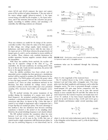
recti®er operation, because negative currents always satisfy FIGURE 12.45 Modulation control methods: (a) periodical sampling;
the inequalities. (b) hysteresis band; and (c) triangular carrier.
With these two stability limits satis®ed, the recti®er will
keep the dc capacitor voltage at the value of V REF (PI maximum value can be evaluated through the following
controller), for all load conditions, by moving power from
equation:
the ac to the dc side. Under inverter operation, the power will
move in the opposite direction. V
Once the stability problems have been solved, and the F S max ¼ D ð12:59Þ
sinusoidal current template has been generated, a modulation 4h L S
method will be required to produce the PWM pattern for the
power valves. The PWM pattern will switch the power valves where h is the magnitude of the hysteresis band.
to force the input currents I_line to follow the desired current The TC method shown in Fig. 12.45c, compares the error
template I_ref. There are many modulation methods in the between I_ref and I_line with a triangular wave. This trian-
literature, but three methods for voltage source current gular wave has ®xed amplitude and frequency and is called the
controlled recti®ers are the most widely used ones: periodical triangular carrier. The error is processed through a propor-
sampling (PS); hysteresis band (HB); and triangular carrier tional-integral (PI) gain stage before comparison with the
(TC). triangular carrier takes place. As can be seen, this control
The PS method switches the power transistors of the scheme is more complex than PS and HB. The values for kp
recti®er during the transitions of a square wave clock of and ki determine the transient response and steady-state error
®xed frequency: the periodical sampling frequency. In each of the TC method. It has been found empirically that the
transition, a comparison between I_ref and I_line is made, and values for kp and ki shown in Eqs. (12.60) and (12.61) give a
corrections take place. As shown in Fig. 12.45a, this type of good dynamic performance under several operating condi-
control is very simple to implement: only a comparator and a tions:
D-type ¯ip-¯op are needed per phase. The main advantage of
this method is that the minimum time between switching L o c
S
kp ¼ ð12:60Þ
transitions is limited to the period of the sampling clock. 2 V D
However, the actual switching frequency is not clearly de®ned.
ki ¼ o kp ð12:61Þ
The HB method switches the transistors when the error c
between I_ref and I_line exceeds a ®xed magnitude: the
hysteresis band. As can be seen in Fig. 12.45b, this type of where L is the total series inductance seen by the recti®er, o c
S
control needs a single comparator with hysteresis per phase. In is the triangular carrier frequency, and V is the dc link voltage
D
this case the switching frequency is not determined, but its of the recti®er.